NCT is adopted for NEDO’s Development of Material Technology for High-Output, High-Efficiency Power Devices / High-Frequency Devices Project
– Development of β-Ga2O3 wafers, power devices and power modules –
Novel Crystal Technology, Inc. (Saitama, Japan, President & CEO: Akito Kuramata, “NCT”) recently announced that a research and development project related to Gallium Oxide Semiconductors was adopted by the New Energy and Industrial Technology Development Organization (NEDO) as their “Development of Material Technology for High-Output and High-Efficiency Power Devices / High-Frequency Devices” as part of “Key and Advanced Technology R&D through Cross Community Collaboration Program” (K Program), promoted by the Cabinet Office (CAO), the Ministry of Education, Culture, Sports, Science and Technology (MEXT), and the Ministry of Economy, Trade and Industry (METI) in Japan.
For this project, NCT will collaborate with Mitsubishi Electric Corporation (Tokyo, Japan) and Japan Fine Ceramics Center (Nagoya, Japan).
With K Program, CAO, MEXT, and METI play a central role across the ministries, in promoting research and development of cutting-edge technologies that are important for economic security. Based on the diversity of science and technology, the program promotes research and development that leads not only to private use but also to public use, and to utilize the results of R&D in cutting-edge important technologies, which would be indispensable for Japan to continue to secure a firm position in the international community in the mid-to-long term.
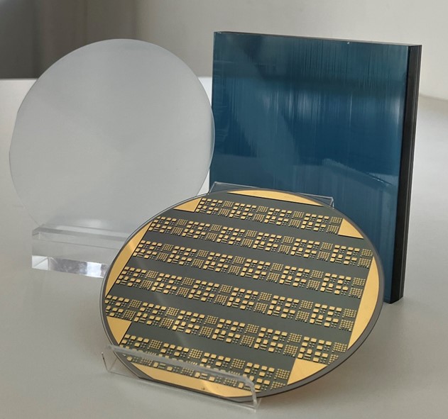
β-Ga2O3 wafers and bulk crystal
Background of our project
With the spread of electric vehicles and renewable energy, and the need to realize next-generation information and communication networks, the realization of power devices*1 that operate at high output and can control electricity in an energy-saving and efficient manner has become an urgent issue. β-Gallium Oxide (β-Ga2O3)*2 shows great value with Baliga’s figure-of-merit*3, which is a performance index for power devices, which is overwhelmingly higher than that of conventional Silicon (Si) semiconductors, and even exceeds Silicon Carbide (SiC)*4, which has been attracting attention in recent years. β-Ga2O3 is expected to realize ultra-low-loss power devices that surpass other materials.
Although Japan is at the forefront of this material field, the potential of β-Ga2O3 has not yet been fully exploited, and it has not yet been realized as a highly productive β-Ga2O3 wafer device.
Details of our project
In this project, we will collaborate with related companies and academic institutions to develop β-Ga2O3 wafers, power devices, and power modules. NCT will work on the development of low-cost crystal growth technology for manufacturing of 6-inch high-quality β-Ga2O3 wafers and 6-inch homoepitaxial growth technology*5 with low defect density and high production throughput. In addition, in collaboration with Mitsubishi Electric Corporation, we will work on the development of a high-voltage β-Ga2O3 transistor with high breakdown voltage at 3.3 kV or more, and low on-resistance which is less than one-half that of SiC. Mitsubishi Electric Corporation will also work on the development of a power module*6 in which multiple β-Ga2O3 transistor chips are assembled in parallel. Japan Fine Ceramics Center will work on the construction of a non-destructive, high-speed full-surface defect inspection technology for 6-inch β-Ga2O3 wafers.
Significance of our project
By achieving the project, we aim to contribute to maintaining the high level of technology in the future. In addition, by utilizing large-diameter, high-quality β-Ga2O3 wafers, high-performance power devices and power modules obtained through this project, we will contribute to the realization of carbon neutrality by responding to the projected increase in power demand in the future, diversifying power facilities, and accelerating the reduction of CO2 emissions in power infrastructure such as renewable energy-related facilities that require high-output operation at high voltages.
Project Period (planned)
5 years from FY2024 to FY2028
Business Budget
4.5 billion yen (maximum)
Business Details
Cabinet Office: “Key and Advanced Technology R&D through Cross Community Collaboration Program”
https://www8.cao.go.jp/cstp/anzen_anshin/kprogram.html (in Japanese)
NEDO: Decision on the implementation structure of the project for “Key and Advanced Technology R&D through Cross Community Collaboration Program / Development of Material Technology for High-Output and High-Efficiency Power Devices / High-Frequency Devices”
https://www.nedo.go.jp/koubo/IT3_100313.html (in Japanese)
Annotation
*1 Power device
A semiconductor device that can control high voltage and current. It is used in power conversion equipment such as inverters.
*2 β-Gallium Oxide (β-Ga2O3)
It is a compound of gallium and oxygen, and is one of the wide-gap semiconductors.
*3 Baliga’s figure of merit
Based on the physical property values of the material, such as electron mobility, dielectric constant, and breakdown electric field strength, it is an index of suitability as a power semiconductor material.
*4 Silicon Carbide (SiC)
It is a compound of silicon and carbon, and is one of the wide-gap semiconductors.
*5 Homoepitaxial growth
Crystal growth of the same substance as the substrate with the same atomic arrangement as the substrate.
*6 Power module
A product combines multiple power devices into a single package.
Contact
Novel Crystal Technology, Inc.
First Research Department
Narikawa
mi.narikawa△novelcrystal.co.jp
*When you contact, please replace “△” with “@”.