- ホーム
- News release
News release
-
 Novel Crystal Technology Achieves Breakthrough in Ga2O3 Crystal Growth, Paving Way for Larger, Higher-Quality Wafers
-
 World’s first inverted gallium oxide DI-MOS transistor
-
 Third-generation gallium-oxide 100-mm epitaxial wafer with ten times fewer killer defects
-
 World’s first successful epitaxial deposition of gallium oxide on a 6-inch wafer using the HVPE method
-
 The world’s first ampere-class 1200-V breakdown-voltage gallium oxide Schottky barrier diode
-
 Gallium oxide vertical transistor with the world’s highest breakdown voltage
-
 High-quality 100-mm β-type gallium oxide epitaxial wafers have been developed.
-
 Development of high-quality β-type gallium oxide film growth technique has been achieved
-
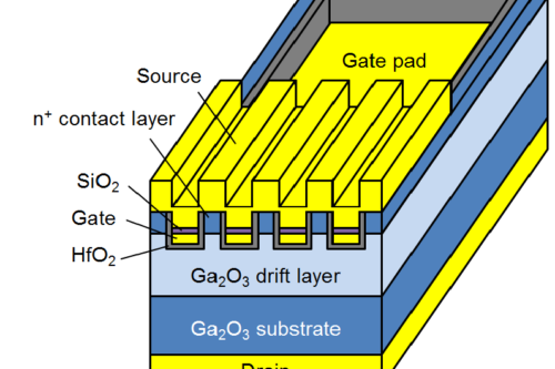
 World’s first successful development of trench MOS type power transistor using gallium oxide epitaxial film
-
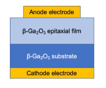
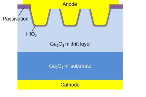
 Successfully developed ultra low power consumption gallium oxide Schottky barrier diode